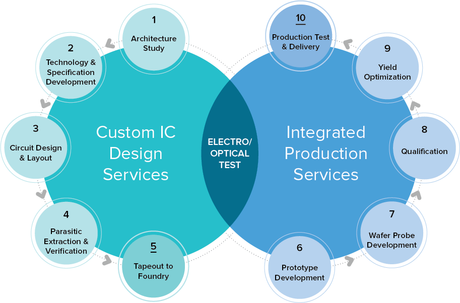
Production Services
Prototype Development
- Package selection and partners for package design
- In-house PCB and test system design services
- Choice of existing test/characterization system re-use or specification and design of new test system
Wafer Probe Development
- Class 100 clean room with 12″ fully automated wafer prober with flexible optical fixture configuration; custom design of probe test program / vectors with optical stimulus available
Qualification
- The Forza Product Engineering Team is on-call for a wide array of Qualification services, including ESD/LU, HTOL, Shock & Vibe, and testing to other JEDEC standards to ensure a high quality, reliable production design
Yield Optimization
- Forza has significant experience taking a design from the lab to production
- Forza will leverage wafer probe development and direct access to Forza Design Engineers to aid in the Integrated Production Services phase of product development
- Detailed knowledge of the design is often the key to making tangible yield improvements and Forza will bring this to bear on your design
- Forza will also take advantage of its foundry relationships to improve yield and design quality in production for our customers
Production Test and Delivery
- Forza has extensive experience transitioning prototype wafer probe & laboratory test programs and equipment to a production-worthy set of test protocols resulting in final product delivery
- The Forza Production Team is on-call for your production test needs